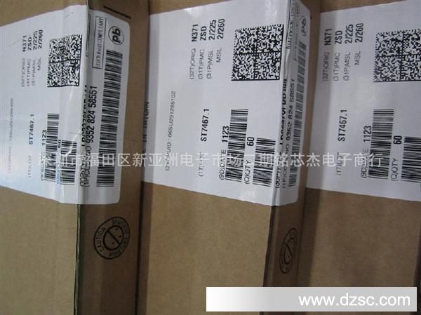
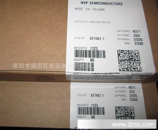
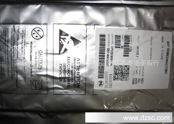
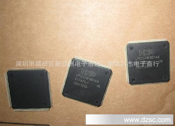
诚信《*十》*批发经销原装*NXP单片机LPC2378FBD144
地区:广东 深圳
认证:
无
图文详情
产品属性
相关推荐
《需要规格书PDF请联系店家哦》
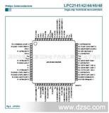
LPC2378
Single-chip 16-bit/32-bit microcontrollers; 512 kB flash with
ISP/IAP, Ethernet, U* 2.0, CAN, and 10-bit ADC/DAC
1. General description
The LPC2378 microcontroller is based on a 16-bit/32-bit ARM7TDMI-S CPU with
real-time emulation that combines the microcontroller with 512 kB of embedded
high-speed flash memory. A 128-bit wide memory interface and a unique accelerator
architecture enable 32-bit code execution at the maximum clock rate. For critical
performance in interrupt service routines and DSP algorithms, this increases performance
up to 30 % over Thumb mode. For critical code size applications, the alternative 16-bit
Thumb mode reduces code by more than 30 % with minimal performance penalty.
The LPC2378 is ideal for multi-purpose serial communication applications. It incorporates
a 10/100 Ethernet Media Access Controller (MAC), U* full speed device with 4 kB of
endpoint RAM, four UARTs, two CAN channels, an SPI interface, two Synchronous Serial
Ports (SSP), three I2C interfaces, an I2S interface, and an External Memory Controller
(EMC). This blend of serial communications interfaces combined with an on-chip 4 MHz
internal oscillator, SRAM of 32 kB, 16 kB SRAM for Ethernet, 8 kB SRAM for U* and
general purpose use, together with 2 kB battery powered SRAM make this device very
well suited for communication gateways and protocol converters. Various 32-bit timers, an
improved 10-bit ADC, 10-bit DAC, PWM unit, a CAN control unit, and up to 104 fast GPIO
lines with up to 50 edge and up to four level sensitive external interrupt pins make these
microcontrollers particularly suitable for industrial control and medical systems.
1。一般描述
LPC2378微控制器的基础上的16-bit/32-bitARM7TDMI-SCPU
实时*,它结合了微控制器,带有512KB的嵌入式
*快闪记忆体。128位宽度的存储器接口和*的加速
结构使32位代码能够在*大时钟速率。对于关键
在中断服务程序和DSP算法的性能,这可以*性能,
Thumb模式的30%以上。对代码规模有严格的应用程序,可使用16位
Thumb模式将代码规模降低*过30%,而性能的损失却很小。
LPC2378是多用途的串行通信应用的理想选择。它集成了
一个10/100以太网媒体访问控制器(MAC),U*全速设备大小为4 KB
端点RAM,4个通用异步收发器(UART),两个CAN通道,一个SPI接口,2个同步串行
端口(SSP),3个I2C接口,I2S接口,和一个外部存储器控制器
(EMC)。这种共混物的串行通信接口结合一个片上的4 MHz
内部振荡器,SRAM,32 KB,16 KBSRAM用于以太网,8 KBSRAM为U*和
一般用途的,再加上2KB电池供电的SRAM使该器件*
*适合于通信网关,协议转换器。多个32位定时器,
改进的10位ADC,10位DAC,PWM单元,CAN控制单元和多达104个快速GPIO
50优势和4个电平触发的外部中断引脚线使这些
微控制器*适用于工业控制和*系统。
2. Features
n ARM7TDMI-S processor, running at up to 72 MHz.
n Up to 512 kB on-chip flash program memory with In-System Programming (ISP) and
In-Application Programming (IAP) capabilities. Flash program memory is on the ARM
local bus for high performance CPU access.
n 32 kB of SRAM on the ARM local bus for high performance CPU access.
n 16 kB SRAM for Ethernet interface. Can also be used as general purpose SRAM.
n 8 kB SRAM for general purpose DMA use also accessible by the U*.
n Dual Advanced High-performance Bus (AHB) system that provides for simultaneous
Ethernet DMA, U* DMA, and program execution from on-chip flash with no
contention between those functions. A bus bridge allows the Ethernet DMA to access
the other AHB subsystem.
n EMC provides support for static devices such as flash and SRAM as well as off-chip
memory mapped peripherals.
n Advanced Vectored Interrupt Controller (VIC), supporting up to 32 vectored interrupts.
n General Purpose AHB DMA controller (GPDMA) that can be used with the SSP serial
interfaces, the I2S port, and the Secure Di*al/MultiMediaCard (SD/MMC) card port,
as well as for memory-to-memory transfers.
LPC2378
Single-chip 16-bit/32-bit microcontrollers; 512 kB flash with
ISP/IAP, Ethernet, U* 2.0, CAN, and 10-bit ADC/DAC
Rev. 01 — 6 December 2006 Preliminary data sheet
LPC2378_1 © NXP B.V. 2006. All rights reserved.
Preliminary data sheet Rev. 01 — 6 December 2006 2 of 54
NXP Semiconductors LPC2378
Fast communication chip
n Serial Interfaces:
u Ethernet MAC with *ociated DMA controller. These functions reside on an
independent AHB bus.
u U* 2.0 full-speed device with on-chip PHY and *ociated DMA controller.
u Four UARTs with fractional baud rate generation, one with modem control I/O, one
with IrDA support, all with FIFO.
u CAN controller with two channels.
u SPI controller.
u Two SSP controllers, with FIFO and multi-protocol capabilities. One is an alternate
for the SPI port, sharing its interrupt and pins. These can be used with the GPDMA
controller.
u Three I2C-bus interfaces (one with open-drain and two with standard port pins).
u I2S (Inter-IC Sound) interface for di*al audio input or output. It can be used with
the GPDMA.
n Other peripherals:
u SD/MMC memory card interface.
u 104 General purpose I/O pins with configurable pull-up/down resistors.
u 10-bit ADC with input multiplexing among 8 pins.
u 10-bit DAC.
u Four general purpose timers/counters with 8 capture inputs and 10 compare
outputs. Each timer block has an external count input.
u One PWM/timer block with support for three-phase motor control. The PWM has
two external count inputs.
u Real-Time Clock (RTC) with separate power pin, clock source can be the RTC
oscillator or the APB clock.
u 2 kB SRAM powered from the RTC power pin, allowing data to be stored when the
rest of the chip is powered off.
u WatchDog Timer (WDT). The WDT can be clocked from the internal RC oscillator,
the RTC oscillator, or the APB clock.
n Standard ARM test/debug interface for compatibility with existing tools.
n Emulation trace module supports real-time trace.
n Single 3.3 V power supply (3.0 V to 3.6 V).
n Four reduced power modes: idle, sleep, power down, and deep power down.
n Four external interrupt inputs configurable as edge/level sensitive. All pins on PORT0
and PORT2 can be used as edge sensitive interrupt sources.
n Processor wake-up from Power-down mode via any interrupt able to operate during
Power-down mode (includes external interrupts, RTC interrupt, U* activity, Ethernet
wake-up interrupt).
n Two independent power domains allow fine tuning of power consumption based on
needed features.
n Each peripheral has its own clock divider for further power saving.
n Brownout detect with separate thresholds for interrupt and forced reset.
n On-chip power-on reset.
n On-chip crystal oscillator with an operating range of 1 MHz to 24 MHz.
n 4 MHz internal RC oscillator trimmed to 1 % accuracy that can optionally be used as
the system clock. When used as the CPU clock, does not allow CAN and U* to run.
LPC2378_1 © NXP B.V. 2006. All rights reserved.
Preliminary data sheet Rev. 01 — 6 December 2006 3 of 54
NXP Semiconductors LPC2378
Fast communication chip
n On-chip PLL allows CPU operation up to the maximum CPU rate without the need for
a high frequency crystal. May be run from the main oscillator, the internal RC
oscillator, or the RTC oscillator.
n Boundary scan for simplified board testing.
n Versatile pin function selections allow more possibilities for using on-chip peripheral
functions.
2。特点
?ARM7TDMI-S处理器,运行速度*72 MHz。
N*高为512 KB片上闪存程序存储器在系统编程(ISP)和
在应用中编程(IAP)功能。闪存程序存储器在ARM
局部总线的*CPU访问。
N 32 KB的SRAM在ARM局部总线的*CPU访问。
N 16 KB SRAM用于以太网接口。也可作为通用SRAM。
N 8 KB SRAM用于通用DMA使用也可以通过U*访问。
n双*的*总线(AHB)系统,提供同步
以太网DMA,U* DMA,并没有从片上闪存程序执行
这些功能之间的争。总线桥允许以太网DMA访问
其它AHB子系统。
?EMC提供支持静态设备(如闪存和SRAM)以及芯片
内存映射的外设。
n*的向量中断控制器(VIC),支持多达32个向量中断。
n一般目的AHB DMA控制器(GPDMA),可用于与SSP串行
接口,I2S端口和*数字/多媒体卡(SD / MMC)卡口,
以及用于存储器到存储器的传输。
LPC2378
单芯片的16-b??it/32-bit微控制器,512 kB闪存
ISP / IAP,以太网,U* 2.0,CAN和10位ADC / DAC
致01 - 于二**六年十二月六日初步数据表
LPC2378_1©NXP B.V.(2006)。保留*权利。
初步数据表致01 - 2006年12月6日2 54
恩智浦LPC2378
快速通信芯片
N个串行接口:
ü相关的DMA控制器,以太网MAC。这些功能驻留在
*的AHB总线。
ü带有片上物理层(PHY)和相关的DMA控制器的U* 2.0全速设备。
ü四个小数波特率发生器的UART,一个与调制解调器控制I / O,1
支持IrDA,*FIFO。
U CAN控制器有两个渠道。
üSPI控制器。
ü2个SSP控制器,带FIFO和多协议功能。一个是备用
SPI端口,共享中断和管脚。这些可用于与GPDMA
控制器。
ü3个I2C总线接口(一个漏*开路和两个标准端口)。
üI2S(IC间音频)接口用于数字音频输入或输出。它可用于
GPDMA。
n其他外设:
üSD / MMC存储卡接口。
×104通用I / O引脚与配置pull-up/down电阻。
U 10位ADC的输入复用8个引脚之间。
U 10位DAC。
ü个通用定时器/计数器,带8路捕获输入和10路比较
输出。每个定时器模块都具有外部计数输入。
U盘PWM /定时器模块,支持三相电机控制。PWM有
两个外部计数输入。
ü实时时钟(RTC)带有*的电源引脚,时钟源可以是RTC
振荡器或APB时钟。
U 2 KB SRAM供电的RTC电源引脚,允许数据存储时,
芯片其余部分的电源已关闭。
ü看门狗定时器(WDT)。WDT可以从内部RC振荡器作为时钟源,
RTC振荡器或APB时钟。
n标准的ARM测试/调试接口,与现有的工具兼容。
?*跟踪模块支持实时跟踪。
n单电源3.3 V(3.0 V至3.6 V)。
?4个低功耗模式:空闲,休眠,断电和深度掉电。
N带四个可配置为边沿/电平触发的外部中断输入。上的*引脚PORT0
PORT2可以作为边沿触发的中断源。
N处理器从掉电模式唤醒操作过程中能够通过任何中断
掉电模式(包括外部中断,RTC中断,U*活动,以太网
唤醒中断)。
n两个*的电源域,允许功耗的基础上微调
所需的功能。
n每个外设都有自己的时钟分频器,以进一步节省电力。
?掉电检测与单独的阈值,中断和强制复位。
n在芯片上电复位。
n在芯片的经营范围为1 MHz到24 MHz晶体振荡器。
N 4 MHz内部RC振荡器可调节到1%的精度,可以有选择地使用
系统时钟。作为CPU时钟时,不允许CAN和U*运行。
LPC2378_1©NXP B.V.(2006)。保留*权利。
初步数据表致01 - 12月6日2006 3 54
恩智浦LPC2378
快速通信芯片
?片上PLL允许的*大CPU速度,而不需要CPU操作
高频晶体。可能会从主振荡器,内部RC
振荡器或RTC振荡器。
简化了电路板测试的的?边界扫描。
?多功能引脚功能选择,让更多的可能性,使用的片上外设
功能。
长期现货供应 支持订货 库存
诚信经销 原装正品 *新年份 *NXP单片机
*配套 欢迎咨询
因为价格有可能会变动哦,请联系店家了解详情后采购。。。

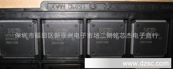
单片机
NXP/恩智浦
LPC2378FBD144
1.5W
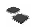
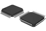
QFP144
QFP144 SOP 贴片
2012+ROHS
16位32位微控制器